


Contact
| Email: | , |
|---|---|
| Website: | http://surfaces.fme.vutbr.cz/research/surfaces-and-interfaces/nanobb/ |
| Phone: | +420 54114 9243 |
| Research group: | Fabrication and Characterisation of Nanostructures - Tomáš Šikola |
| Workplace: |
20. May 2020
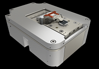
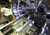
Vědci z několika institucí otevřou nové možnosti mikroskopického zkoumání materiálů
Další posun v mikroskopickém zkoumání materiálů pomocí inovovaného zařízení LiteScope, který vyvinula a vyrábí brněnská společnost NenoVision,…
20. May 2020
Vědci otevřou nové možnosti mikroskopického zkoumání materiálů
Další posun v mikroskopickém zkoumání materiálů pomocí inovovaného zařízení LiteScope, který vyvinula a vyrábí brněnská společnost NenoVision, je…
Publications that are part of the Web of Science database, possibly also other publications chosen by authors.
2021
- Backes, C., Bartus, S., Casiraghi, C., Ferrari, A., Kamali, A.R., Kolíbal, M., Kumar, V., Molle, A., Oyarzun, A., Palermo, V., Sengupta, A., Silvestri, A., Zhang, H., , 2021: Applications in opto-electronics: general discussion. FARADAY DISCUSSIONS OF THE CHEMICAL SOCIETY , p. 184 - 5, doi: 10.1039/D1FD90006D; FULL TEXT
-
NAZZARI, D., GENZER, J., RITTER, V., BETHGE, O., BERTAGNOLLI, E., RAMER, G., LENDL, B., WATANABE, K., TANIGUCHI, T., RURALI, R., KOLÍBAL, M., LUGSTEIN, A., 2021: Highly Biaxially Strained Silicene on Au(111). JOURNAL OF PHYSICAL CHEMISTRY C (WEB) 125(18), p. 9973 - 8, doi: 10.1021/acs.jpcc.0c11033; FULL TEXT
(UHV-LEEM, UHV-MBE, UHV-DEPOSITION) - Backes, C., Bianco, A., Casiraghi, C., Galembeck, F., Gupta, R.K., Hersam, M.C., Kamali, A.R., Kolíbal, M., Kolosov, V., Kumar, V., Lee, W. H., Martsinovich, N., Melchionna, M., Mullen, K., Oyarzun, A., Palermo, V., Prato, M., Samori, P., Sampath, S., Silvestri, A., Sirbu, D., Sui, R.H., Turchanin, A., Wetzl, C., Wright, I.A., Xia, Z.Y., Zhuang, X.D. , 2021: 2D materials production and generation of functional inks: general discussion. FARADAY DISCUSSIONS OF THE CHEMICAL SOCIETY , p. 141 - 22, doi: 10.1039/D1FD90002A; FULL TEXT
2020
- WANG, Y.; ŠIKOLA, T.; KOLÍBAL, M., 2020: Collector Droplet Behavior during Formation of Nanowire Junctions. J PHYS CHEM LETT 11(16), p. 6498 - 7, doi: 10.1021/acs.jpclett.0c01653; FULL TEXT
-
WANG, T.; SHI, Y.; PUGLISI, F. M.; CHEN, S.; ZHU, K.; ZOU, Y.; LI, X.; JING, X.; HAN, T.; GUO, B.; BUKVIŠOVÁ, K.; KACHTÍK, L.; KOLÍBAL, M.; WEN, CH.; LANZA, M., 2020: Electroforming in Metal-Oxide Memristive Synapses. ACS APPLIED MATERIALS & INTERFACES 12(10), p. 11806 - 9, doi: 10.1021/acsami.9b19362; FULL TEXT
(TITAN, HELIOS)
2019
- VOBORNÝ, S.; MÜNZ, F.; KOLÍBAL, M., 2019: Metal-nitridová vrstva s plazmonickou optickou strukturou. ; FULL TEXT
- MACH, J.; KOLÍBAL, M., 2019: Ovládací jednotka pro zdroj atomárního vodíku. ; FULL TEXT
- KOLÍBAL, M.; DHANKHAR, M.; BUKVIŠOVÁ, K.; NOVÁK, L., 2019: Verified technology for utilization of atomic hydrogen source in SEM. ; FULL TEXT
-
KOLÍBAL, M.; BUKVIŠOVÁ, K.; KACHTÍK, L.; ZAK, A.; NOVÁK, L.; ŠIKOLA, T., 2019: Formation of Tungsten Oxide Nanowires by Electron-Beam-Enhanced Oxidation of WS2 Nanotubes and Platelets. JOURNAL OF PHYSICAL CHEMISTRY C (PRINT) 123(14), p. 9552 - 8, doi: 10.1021/acs.jpcc.9b00592; FULL TEXT
(TITAN, VERIOS, KRATOS-XPS) -
NOVÁK, T.; KOSTELNÍK, P.; KONEČNÝ, M.; ČECHAL, J.; KOLÍBAL, M.; ŠIKOLA, T., 2019: Temperature effect on Al predose and AlN nucleation affecting the buffer layer performance for the GaN-on-Si based high-voltage devices. JAPANESE JOURNAL OF APPLIED PHYSICS 58, p. SC1018-1 - 9, doi: 10.7567/1347-4065/ab0d00; FULL TEXT
(ICON-SPM, KRATOS-XPS)
2018
-
KOLÍBAL, M.; PEJCHAL, T.; MUSÁLEK, T.; ŠIKOLA, T., 2018: Catalyst–substrate interaction and growth delay in vapor–liquid–solid nanowire growth. NANOTECHNOLOGY 29(20), p. 1 - 7, doi: 10.1088/1361-6528/aab474; FULL TEXT
(NANOSAM, VERIOS) - MACH, J.; KOLÍBAL, M.; MUSÁLEK, T., 2018: Funkční vzorek zdroje atomárního vodíku pro SEM. ; FULL TEXT
2017
-
JIANG, L.; XIAO, N.; WANG, B.; GRUSTAN-GUTIERREZ, E.; JING, X.; BÁBOR, P.; KOLÍBAL, M.; LU, G.; WU, T.; WANG, H.; HUI, F.; SHI, Y.; SONG, B.; XIE, X.; LANZA, M., 2017: High-resolution characterization of hexagonal boron nitride coatings exposed to aqueous and air oxidative environments. NANO RESEARCH 10(6), p. 2046 - 10, doi: 10.1007/s12274-016-1393-2; FULL TEXT
(NANOSAM, SIMS)
2016
- DVOŘÁK, P.; KOLÍBAL, M.; SPOUSTA, J.; ŠIKOLA, T., 2016: Fotoluminiscence h-BN detekována pomocí rastrovací optické mikroskopie v blízkém poli. JEMNÁ MECHANIKA A OPTIKA , p. 149 - 2; FULL TEXT
-
KOLÍBAL, M.; PEJCHAL, T.; VYSTAVĚL, T.; ŠIKOLA, T., 2016: The Synergic Effect of Atomic Hydrogen Adsorption and Catalyst Spreading on Ge Nanowire Growth Orientation and Kinking. NANO LETTERS 16(8), p. 4880 - 7, doi: 10.1021/acs.nanolett.6b01352; FULL TEXT
(NANOSAM, TITAN) -
ELBADAWI, C.; TRAN, T.; KOLÍBAL, M.; ŠIKOLA, T.; SCOTT, J.; CAI, Q.; LI, L.; TANIGUCHI, T.; WATANABE, K.; TOTH, M.; AHARONOVICH, I.; LOBO, C., 2016: Electron beam directed etching of hexagonal boron nitride. NANOSCALE 8(36), p. 16182 - 5, doi: 10.1039/c6nr04959a; FULL TEXT
(NANOSAM) - KOLÍBAL, M.; NOVÁK, L.; SHANLEY, T.; TOTH, M.; ŠIKOLA, T., 2016: Silicon oxide nanowire growth mechanisms revealed by real-time electron microscopy. NANOSCALE 8(1), p. 266 - 10, doi: 10.1039/C5NR05152E; FULL TEXT
2014
- KOLÍBAL, M.; PEJCHAL, T.; ŠIKOLA, T., 2014: One-dimensional nanostructures for detection of biomolecules. , p. 152 - 1; FULL TEXT
- LIGMAJER, F.; DRUCKMÜLLEROVÁ, Z.; MĚCH, R.; KOLÍBAL, M.; ŠIKOLA, T., 2014: Tvorba uspořádaných souborů kovových nanočástic na polovodičových substrátech a jejich charakterizace pomocí spektroskopické elipsometrie. , p. 178 - 3; FULL TEXT
- DRUCKMÜLLEROVÁ, Z.; KOLÍBAL, M.; VYSTAVĚL, T.; ŠIKOLA, T., 2014: Toward Site-Specific Dopant Contrast in Scanning Electron Microscopy. MICROSCOPY AND MICROANALYSIS 20(4), p. 1312 - 6, doi: 10.1017/S1431927614000968; FULL TEXT
- KOLÍBAL, M.; VYSTAVĚL, T.; VARGA, P.; ŠIKOLA, T., 2014: Real-Time Observation of Collector Droplet Oscillations during Growth of Straight Nanowires. NANO LETTERS 14(4), p. 1756 - 6, doi: 10.1021/nl404159x; FULL TEXT
- MACH, J.; ŠAMOŘIL, T.; KOLÍBAL, M.; ZLÁMAL, J.; VOBORNÝ, S.; BARTOŠÍK, M.; ŠIKOLA, T., 2014: Optimization of ion-atomic beam source for deposition of GaN ultrathin films. REVIEW OF SCIENTIFIC INSTRUMENTS 85(8), p. 083302-1 - 5, doi: 10.1063/1.4892800; FULL TEXT
2012
- KOLÍBAL, M.; KALOUSEK, R.; NOVÁK, L.; VYSTAVĚL, T.; ŠIKOLA, T., 2012: Controlled faceting in (110) germanium nanowire growth by switching between vapor-liquid-solid and vapor-solid-solid growth. APPLIED PHYSICS LETTERS 100(20), p. 203102-1 - 4, doi: 10.1063/1.4714765; FULL TEXT
- KOLÍBAL, M.; KONEČNÝ, M.; LIGMAJER, F.; ŠKODA, D.; VYSTAVĚL, T.; ZLÁMAL, J.; VARGA, P.; ŠIKOLA, T., 2012: Guided Assembly of Gold Colloidal Nanoparticles on Silicon Substrates Prepatterned by Charged Particle Beams. ACS NANO 6(11), p. 10098 - 9, doi: 10.1021/nn3038226; FULL TEXT
2011
- Kolibal, M; Matlocha, T; Vystavel, T; Sikola, T, 2011: Low energy focused ion beam milling of silicon and germanium nanostructures. NANOTECHNOLOGY 22(10), doi: 10.1088/0957-4484/22/10/105304
- KOLÍBAL, M.; VYSTAVĚL, T.; NOVÁK, L.; MACH, J.; ŠIKOLA, T., 2011: In-situ observation of <110> oriented Ge nanowire growth and associated collector droplet behavior. APPLIED PHYSICS LETTERS 99(14), p. 143113-1 - 3, doi: 10.1063/1.3647774; FULL TEXT
- MACH, J.; ŠAMOŘIL, T.; VOBORNÝ, S.; KOLÍBAL, M.; ZLÁMAL, J.; SPOUSTA, J.; DITTRICHOVÁ, L.; ŠIKOLA, T., 2011: An ultra-low energy (30–200 eV) ion-atomic beam source for ion-beam-assisted deposition in ultrahigh vacuum. , p. 083302-1 - 7; FULL TEXT
- Mach, J; Samoril, T; Voborny, S; Kolibal, M; Zlamal, J; Spousta, J; Dittrichova, L; Sikola, T, 2011: An ultra-low energy (30-200 eV) ion-atomic beam source for ion-beam-assisted deposition in ultrahigh vacuum. REVIEW OF SCIENTIFIC INSTRUMENTS 82(8), doi: 10.1063/1.3622749
2010
- Kolibal, M; Cechal, J; Bartosik, M; Mach, J; Sikola, T, 2010: Stability of hydrogen-terminated vicinal Si(111) surface under ambient atmosphere. APPLIED SURFACE SCIENCE 256(11), p. 3423 - 3426, doi: 10.1016/j.apsusc.2009.12.045
- Cechal, J; Polcak, J; Kolibal, M; Babor, P; Sikola, T, 2010: Formation of copper islands on a native SiO2 surface at elevated temperatures. APPLIED SURFACE SCIENCE 256(11), p. 3636 - 3641, doi: 10.1016/j.apsusc.2009.12.168
- Matlocha, T; Prusa, S; Kolibal, M; Babor, P; Primetzhofer, D; Markin, SN; Bauer, P; Sikola, T, 2010: A study of a LEIS azimuthal scan behavior: Classical dynamics simulation. SURFACE SCIENCE 604(21-22), p. 1906 - 1911, doi: 10.1016/j.susc.2010.07.026
2009
- Bartosik, M; Kolibal, M; Cechal, J; Mach, J; Sikola, T, 2009: Selective Growth of Metallic Nanostructures on Surfaces Patterned by AFM Local Anodic Oxidation. JOURNAL OF NANOSCIENCE AND NANOTECHNOLOGY 9(10), p. 5887 - 5890
- Cechal, J; Tomanec, O; Skoda, D; Konakova, K; Hrncir, T; Mach, J; Kolibal, M; Sikola, T, 2009: Selective growth of Co islands on ion beam induced nucleation centers in a native SiO(2) film. JOURNAL OF APPLIED PHYSICS 105(8)
- Cechal, J; Matlocha, T; Polcak, J; Kolibal, M; Tomanec, O; Kalousek, R; Dub, P; Sikola, T, 2009: Characterization of oxidized gallium droplets on silicon surface: An ellipsoidal droplet shape model for angle resolved X-ray photoelectron spectroscopy analysis. THIN SOLID FILMS 517(6), p. 1928 - 1934
- Nanotechnologies and novel materials II. (CEITEC VUT-S-20-6421), VUT v Brně, 2020 - 2023
- Centrum elektronové a fotonové optiky (TN01000008), Technologická agentura ČR, Technology Agency of the Czech Republic, 2018 - 2022
- Advanced imaging of nanoscale materials in SEM (TN01000008/10), Technologická agentura ČR, Technology Agency of the Czech Republic, 2019 - 2022
- Advanced optical methods for form and surface measurements (TN01000008/21), TA ČR, 2018 - 2022
- Influence of grain boundaries and defects in WS2 nanotubes on their electrical properties. (CEITEC VUT-J-21-7372), VUT v Brně, 2021 - 2022
- Výzkum a vývoj objemových polovodičových materiálů s velkou šířkou zakázaného pásu (TH03020005), Technologická agentura ČR, Technology Agency of the Czech Republic, 2018 - 2020
- AMISPEC_Platforma pokročilých mikroskopických a spektroskopických technik pro nano a mikrotechnologie (TE01020233), TA ČR, 2012 - 2019
- Vývoj atomárního zdroje pro aplikace v elektronové mikroskopii (TJ01000271), Technologická agentura ČR, Technology Agency of the Czech Republic, 2018 - 2019
- Manufacture of magnetic metamaterials using a direct entry focused ion beam (GA15-62503S), Czech Science Foundation - International Projects, 2015 - 2017
- Self-organized functional layers of molecular quantum bits (7AMDE005), DAAD, 2015 - 2016
- Growth of semiconductor nanofibres with optimized functional properties (GPP108/12/P699), Grantová agentura ČR, Czech Science Foundation, 2012 - 2014
- Fabrication of semiconductor nanowires with optimized functional properties (GPP108/12/P699), Czech Science Foundation - Postdoc Grants, 2012 - 2014
- Fabrication of metallic nanostructures for spintronic applications (GPP102/12/P443), Czech Science Foundation - Postdoc Grants, 2012 - 2014
- Mapping of localized plasmon resonances at nanoantennas (GAP102/12/1881), Czech Science Foundation - Standard Grants, 2012 - 2014
I welcome applications from motivated students who would like to work on topics related to my research interests. Please check out group webpage.
Topics for the next academic year:
1. Catalytic growth of selected III-V semiconductor nanowires
The study will be aimed at the growth of III-Sb and III-As nanowires utilizing various catalyst nanoparticles in a MBE chamber of the complex UHV system in CEITEC Nano research infrastructure. Characterization of morphology, composition, and structure, as well as measurement of their optical and electrical transport properties will serve as tools for monitoring the quality of nanowires for electronic and plasmonic applications. The PhD candidate will be focused mostly on fundamental research, explaining processes and mechanisms happening during the nanowire growth.
2. Fabrication of nanowire based devices for use in nanophotonics or bio-intefaces
Due to their geometry, one-dimensional materials seem to be natural building blocks for many device systems, e.g. in electronics or photonics. They can be easily and reproducibly contacted and allow to design 3D devices. Additionally, they seem to be natural choice for nanoscale electrodes (e.g. for detecting cells signalling) or for nanoscale-patterned macroscale electrodes (e.g. in electrochemistry). Currently, mostly undergraduates in our group deal with lithography, which is necessary for device design. We seek for a PhD candidate capable of fabricating a device geometry on demand, and aiming at performing measurements (electrical, optical) relevant for the device application (photonics, bio interfacing, sensing etc.).
3. In-situ monitoring of nanostructures growth
Revealing the growth mechanisms at nanoscale is particularly challenging from many reasons. The most prominent advances in physics of nanostructure growth were achieved utilizing real-time in-situ monitoring techniques (both microscopic and spectroscopic). In our group, we have a large expertise in real time electron microscopy and, in the following year, we will install a new vacuum chamber dedicated to Fourier transform Infrared spectroscopy. The aim of this PhD dissertation is to work on revealing puzzling growth modes of different nanostructures of interest (semiconductor nanowires grown by MBE, metallic/oxide threedimensional nanostructures formed by Focused Electron Beam Induced Deposition etc.) utilizing state-of-the-art equipment. Close collaboration with ThermoFisher Scientific R&D labs will be part of applicants work.