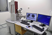
Scanning electron microscope (SEM) MIRA3 XMU (MIRA3-XMU)
Guarantor:
Petr Lepcio, Ph.D.
Instrument status:
![]() Operational, 16.8.2021 10:47, Stage fixed
Operational, 16.8.2021 10:47, Stage fixed
Equipment placement:
CEITEC Nano - A1.11
Research group:
CF: CEITEC Nano
Detailed description:
Scanning electron microscope (SEM) MIRA3 XMU
Description
• Scanning electron microscope (SEM) is used to study the morphology and topography of conductive and non-conductive materials in high resolution (micro to nano-scale).
• Observation of surface samples with high depth of focus using multiple detection system (SE, BSE, STEM) including elemental analysis using energy dispersive spectrometer (EDS).
Acessory: Sputtering and Carbon Thread Coater Leica EM ACE600 for coating non-conductive material with a thin layer (thickness in nanometers) of conductive material.
• carbon coating and high vacuum sputtering of metals (gold, platinum, titanium, gold/palladium)
• integrated measurement of coating thickness based on the QCM crystal with an accuracy of 0.1 nm
• plasma cleaning of the sample and the interior part of equipment
Applications
• Observation both the surface and internal structure of micro and nano-objects (phase interface such as matrix-filler/reinforcement, particle distribution, aggregates and defects, fracture surfaces, porous 3D materials, units of supramolecular structure and so on)
• evaluation of the shape and dimensions (length, diameter, volume, roughness) of powders, tubes, short fibers
• fast and highly accurate chemical microanalysis and elemental mapping of a sample surface
• qualitative elemental analysis including determination of the distribution of each element
• quantitative analysis of the individual elements in a sample
• The structural analysis of polymeric materials, biopolymers and composites, biomaterials, ceramics, bones, teeth, substrates for tissue engineering, etc.
Specification
• High Brightness Schottky Emitter
• Detectors:
SE, BSE, In-beam SE, In-Beam BSE
LVSTD
STEM detector
EDX analysis
• High-vacuum (≤9x10⁻³Pa) or low-vacuum mode (7-500 Pa)
• Magnification 25 to 1 000 000x
• Acceleration voltage 200 V to 30 kV
• X-Y-Z 130×130×100mm
• Maximum specimen height: 106 mm
Publications:
-
Urso, M.; Ussia, M.; Pumera, M., 2021: Breaking Polymer Chains with Self‐Propelled Light‐Controlled Navigable Hematite Microrobots. ADVANCED FUNCTIONAL MATERIALS 31(28), doi: 10.1002/adfm.202101510; FULL TEXT
(MIRA3-XMU, KRATOS-XPS, RIGAKU9) -
ZBONČÁK, M.; ONDREÁŠ, F.; UHLÍŘ, V.; LEPCIO, P.; MICHALIČKA, J.; JANČÁŘ, J., 2020: Translation of segment scale stiffening into macro scale reinforcement in polymer nanocomposites. POLYMER ENGINEERING AND SCIENCE 60(3), p. 587 - 10, doi: 10.1002/pen.25317; FULL TEXT
(MIRA3-XMU, FISCHIONE-TEM MILL) -
NOVOTNÁ, V., HORÁK, J., KONEČNÝ, M., HEGROVÁ, V., NOVOTNÝ, O., NOVÁČEK, Z., NEUMAN, J., 2020: AFM-in-SEM as a Tool for Comprehensive Sample Surface Analysis. MICROSCOPY TODAY , p. 38 - 9, doi: 10.1017/S1551929520000875; FULL TEXT
(MIRA3-XMU, LITESCOPE)