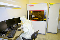
UV Direct Write Laser system Heidelberg Instruments DWL 66-fs (DWL)
CONTACT US
Guarantor:
Radim Zahradníček, Ph.D.
Technology / Methodology:
Nanolitography infrastructure
Instrument status:
 Some Issues, 9.9.2021 15:29, Writing speed is 3 times slower, please count with it during your exposition. This issue is now discuss with service.
Equipment placement:
CEITEC Nano - C1.29
Research group:
CF: CEITEC Nano
Detailed description:
The DWL 66FS laser lithography system is a high resolution pattern generator for low volume mask making and direct writing. The capabilities and flexibility of this system allows to use this research tool in MEMS, BioMEMS, Micro Optics, ASICs, Micro Fluidics, Sensors, CGHs, and all other applications that require microstructures. It can be used for mask making or direct exposure on basically any flat material coated with photoresist. Numerous optional features increase the flexibility and make the system suitable for more applications. If one of your applications requires a special technology, it can most likely be implemented in the DWL 66FS. The system can utilize a variety of different lasers, which makes it possible to expose nearly all photoresists, including UV resists like SU8. In addition to high resolution 2D patterns, it is also possible to create complex 3D structures in thick photoresist with a single pass. By supporting five different write modes the resolution and throughput of the system can be optimized for each application. The optional vector exposure mode will offer even further flexibility such as improved structure quality and a higher throughput for certain designs like waveguides or microfluidic channels. To ensure the stability of the system, it is placed in a climate chamber providing a constant temperature. The optical setup, the autofocus system and the high precision stage system guarantee the quality of the exposed structures. During operation a high resolution interferometer controls the position of the stage with high accuracy. All this allows the system to write structures down to 0.6 μm with an address grid of 50 nm. The DWL 66FS includes two CCD cameras used for metrology and alignment purposes. This enables the system to perform overlay exposures with high accuracy. Arbitrary structures on the substrate can be used for the alignment. The optional backside alignment system uses two additional cameras to align front side exposures to structures on the back side of the substrate.
Publications:
-
GABLECH, I.; BRODSKÝ, J.; PEKÁREK, J.; NEUŽIL, P., 2020: Infinite selectivity of wet SiO2 etching in respect to Al . MICROMACHINES 11(4), p. 365 - 7, doi: 10.3390/mi11040365; FULL TEXT
(EVAPORATOR, SUSS-MA8, RIE-CHLORINE, DWL, SUSS-RCD8)
-
Chmela, O., 2020: Progress toward the development of single nanowire-based arrays for gas sensing applications. PH.D THESIS , p. 1 - 199
(ALD, DWL, KAUFMAN, DIENER, SUSS-MA8, SUSS-RCD8, RAITH, MAGNETRON, EVAPORATOR, RIE-FLUORINE, SCIA, DEKTAK, ICON-SPM, NANOCALC, MPS150, WIRE-BONDER)
-
BARTOŠÍK, M.; MACH, J.; PIASTEK, J.; NEZVAL, D.; KONEČNÝ, M.; ŠVARC, V.; ENSSLIN, K.; ŠIKOLA, T., 2020: Mechanism and Suppression of Physisorbed-Water-Caused Hysteresis in Graphene FET Sensors. ACS SENSORS 5(9), p. 2940 - 10, doi: 10.1021/acssensors.0c01441; FULL TEXT
(EVAPORATOR, DWL, DIENER)
-
LIU, X.; FECKO, P.; FOHLEROVÁ, Z.; PEKÁREK, J.; KARÁSEK, T.; NEUŽIL, P., 2020: Parylene Micropillars Coated with Thermally Grown SiO2. JOURNAL OF VACUUM SCIENCE & TECHNOLOGY B 38(6), p. 38 - 6, doi: 10.1116/6.0000558; FULL TEXT
(SUSS-MA8, SUSS-RCD8, DWL, DRIE, RIE-FLUORINE, PARYLENE, XEF2, APCVD, LYRA)
-
Brodský, J., 2019: Characterization of graphene elecrical properties on MEMS structures. BACHELOR´S THESIS , p. 1 - 50
(MPS150, WITEC-RAMAN, EVAPORATOR, DRIE, PECVD, DWL, SUSS-MA8, RIE-FLUORINE, RIE-CHLORINE, DIENER, SCIA)
-
Fecko, P., 2019: Gecko mimicking surfaces. MASTER´S THESIS , p. 1 - 52
(SUSS-RCD8, SUSS-MA8, DWL, DRIE, LYRA, ALD, RIE-FLUORINE, ICON-SPM, PARYLENE, XEF2)
-
GABLECH, I.; KLEMPA, J.; PEKÁREK, J.; VYROUBAL, P.; KUNZ, J.; NEUŽIL, P., 2019: Aluminum nitride based piezoelectric harvesters. 2019 19TH INTERNATIONAL CONFERENCE ON MICRO AND NANOTECHNOLOGY FOR POWER GENERATION AND ENERGY CONVERSION APPLICATIONS (POWERMEMS) (001), p. 1 - 4, doi: 10.1109/PowerMEMS49317.2019.82063211368; FULL TEXT
(DIENER, DRIE, DWL, KAUFMAN, RIE-CHLORINE, SUSS-MA8)
-
HRDÝ, R.; PRÁŠEK, J.; FILLNER, P.; VANČÍK, S.; SCHNEIDER, M.; HUBÁLEK, J.; SCHMID, U., 2019: Development of HfO2/Al2O3 Stack for On-Chip Capacitor Applications
. INTERNATIONAL SPRING SEMINAR ON ELECTRONICS TECHNOLOGY ISSE , p. 1 - 4, doi: 10.1109/ISSE.2019.8810156; FULL TEXT
(ALD, SUSS-MA8, EVAPORATOR, SUSS-RCD8, DWL, RIE-CHLORINE)
-
PRÁŠEK, J.; HOUŠKA, D.; HRDÝ, R.; HUBÁLEK, J.; SCHMID, U., 2019: Optimization of Cryogenic Deep Reactive Ion Etching Process for On-Chip Energy Storage
. INTERNATIONAL SPRING SEMINAR ON ELECTRONICS TECHNOLOGY ISSE , p. 1 - 6, doi: 10.1109/ISSE.2019.8810293; FULL TEXT
(DRIE, ICON-SPM, SUSS-MA8, SUSS-RCD8, EVAPORATOR, DWL)
-
CHMELA, O.; SADÍLEK, J.; SAMA, DOMENECH-GIL, G.; J.; SOMER, J.; MOHAN, R.; ROMANO-RODRIGUEZ, A.; HUBÁLEK, J.; VALLEJOS VARGAS, S., 2018: Selectively arranged single-wire based nanosensor array systems for gas monitoring. NANOSCALE 10(19), p. 9087 - 10, doi: 10.1039/c8nr01588k; FULL TEXT
(RAITH, DWL, KAUFMAN, MAGNETRON, SCIA, RIE-FLUORINE, WIRE-BONDER, RIGAKU3)
-
PODEŠVA, P.; GABLECH, I.; NEUŽIL, P., 2018: Nanostructured Gold Microelectrode Array for Ultrasensitive Detection of Heavy Metal Contamination. ANALYTICAL CHEMISTRY 90(2), p. 1161 - 7, doi: 10.1021/acs.analchem.7b0372; FULL TEXT
(SUSS-MA8, DWL, SCIA, DIENER)
-
STARÁ, V.; PROCHÁZKA, P.; MAREČEK, D.; ŠIKOLA, T.; ČECHAL, J., 2018: Ambipolar remote graphene doping by low-energy electron beam irradiation. NANOSCALE 10(37), p. 17520 - 5, doi: 10.1039/c8nr06483k; FULL TEXT
(ALD, DIENER, DWL, EVAPORATOR)
-
GABLECH, I.; SOMER, J.; FOHLEROVÁ, Z.; SVATOŠ, V.; PEKÁREK, J.; KURDÍK, S.; FENG, J.; FECKO, P.; PODEŠVA, P.; HUBÁLEK, J.; NEUŽIL, P., 2018: Fabrication of buried microfluidic channels with observation windows using femtosecond laser photoablation and parylene-C coating. MICROFLUIDICS AND NANOFLUIDICS 22(9), p. NA - 7, doi: 10.1007/s10404-018-2125-6; FULL TEXT
(DRIE, DWL, SUSS-MA8, PARYLENE, XEF2)
-
Vančík, S., 2018: MEMS microhotplate platform for chemical sensors. MASTER´S THESIS , p. 1 - 68
(DWL, ALD, MAGNETRON, EVAPORATOR, RIE-FLUORINE, SUSS-MA8, DEKTAK, MPS150, RIE-CHLORINE)
-
MACH, J.; PROCHÁZKA, P.; BARTOŠÍK, M.; NEZVAL, D.; PIASTEK, J.; HULVA, J.; ŠVARC, V.; KONEČNÝ, M.; KORMOŠ, L.; ŠIKOLA, T., 2017: Electronic transport properties of graphene doped by gallium. NANOTECHNOLOGY 28(41), p. 1 - 10, doi: 10.1088/1361-6528/aa86a4; FULL TEXT
(DIENER, DWL, EVAPORATOR, WIRE-BONDER, LYRA)
-
VAŇATKA, M.; URBÁNEK, M.; JÍRA, R.; FLAJŠMAN, L.; DHANKHAR, M.; IM, M.; MICHALIČKA, J.; UHLÍŘ, V.; ŠIKOLA, T., 2017: Magnetic vortex nucleation modes in static magnetic fields. AIP ADVANCES 7(10), p. 1 - 8, doi: 10.1063/1.5006235; FULL TEXT
(DWL, EVAPORATOR, RAITH, TITAN, WIRE-BONDER)
-
Chmela, O; Sadilek, J; Sama, J; Romano-Rodriguez, A; Hubalek, J; Vallejos, S, 2017: Nanosensor array systems based on single functional wires selectively integrated and their sensing properties to C2H6O and NO2. NANOTECHNOLOGY VIII 10248, doi: 10.1117/12.2265000
(RAITH, DWL, KAUFMAN, SCIA, RIE-FLUORINE, MAGNETRON, RIGAKU3)
-
CHMELA, O.; SADÍLEK, J.; VALLEJOS VARGAS, S.; HUBÁLEK, J., 2017: Microelectrode array system as platforms for single nanowire based sensors . JOURNAL OF ELECTRICAL ENGINEERING
68(2), p. 158 - 5, doi: 10.1515/jee-2017-0023; FULL TEXT
(DWL, KAUFMAN, MPS150, RIGAKU3)
-
Citterberg, D., 2017: Preparation of contacts to one-dimensional nanostructurs. BACHELOR´S THESIS , p. 1 - 26
(DWL, MIRA, WIRE-BONDER, EVAPORATOR)
-
Lišková, Z., 2015: Fabrication of Nanostructures and Nanodevices for Nanoelectronics and Spintronics. PH.D. THESIS , p. 1 - 106
(LYRA, MIRA, DIENER, NANOCALC, DWL, EVAPORATOR, WIRE-BONDER, ALD)
Show more publications...
 CEITEC BUT